Product Summary
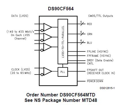
The DS90CF564MTD transmitter converts 21 bits of CMOS/TTL data into three LVDS (Low Voltage Differential Signaling) data streams. A phase-locked transmit clock is transmitted in parallel with the data streams over a fourth LVDS link. Every cycle of the DS90CF564MTD clock 21 bits of input data are sampled and transmitted.
Parametrics
DS90CF564MTD absolute maximum ratings: (1)Supply Voltage (VCC): -0.3V to +6V; (2)CMOS/TTL Input Voltage: -0.3V to (VCC + 0.3V); (3)CMOS/TTL Output Voltage: -0.3V to (VCC + 0.3V); (4)LVDS Receiver Input Voltage: -0.3V to (VCC + 0.3V); (5)Junction Temperature: +150℃; (6)Storage Temperature: -65℃ to +150℃; (7)Lead Temperature (Soldering, 4 sec): +260℃.
Features
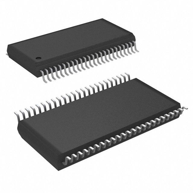
DS90CF564MTD features: (1)20 to 65 MHz shift clk support; (2)Up to 171 Mbytes/s bandwidth; (3)Cable size is reduced to save cost; (4)290 mV swing LVDS devices for low EMI; (5)Low power CMOS design (< 550 mW typ); (6)Power-down mode saves power (< 0.25 mW); (7)PLL requires no external components; (8)Low profile 48-lead TSSOP package; (9)Falling edge data strobe; (10)Compatible with TIA/EIA-644 LVDS standard; (11)Single pixel per clock XGA (1024 x 768); (12)Supports VGA, SVGA, XGA and higher; (13)1.3 Gbps throughput.
Diagrams

| Image | Part No | Mfg | Description |  |
Pricing (USD) |
Quantity | ||||||||||||
|---|---|---|---|---|---|---|---|---|---|---|---|---|---|---|---|---|---|---|
 |
 DS90CF564MTD |
 National Semiconductor (TI) |
 LVDS Interface IC |
 Data Sheet |

|
|
||||||||||||
 |
 DS90CF564MTD/NOPB |
 National Semiconductor (TI) |
 LVDS Interface IC |
 Data Sheet |

|
|
||||||||||||
 |
 DS90CF564MTDX/NOPB |
 National Semiconductor (TI) |
 LVDS Interface IC |
 Data Sheet |

|
|
||||||||||||
 |
 DS90CF564MTDX |
 National Semiconductor (TI) |
 LVDS Interface IC |
 Data Sheet |

|
|
||||||||||||
 (China (Mainland))


