Product Summary
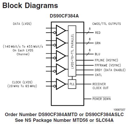
The DS90CF384AMTD receiver converts the four LVDS data streams (Up to 1.8 Gbps throughput or 227 Megabytes/sec bandwidth) back into parallel 28 bits of CMOS/TTL data (24 bits of RGB and 4 bits of Hsync, Vsync, DE and CNTL).
Parametrics
DS90CF384AMTD absolute maximum ratings: (1)Supply Voltage (VCC): -0.3V to +4V; (2)CMOS/TTL Input Voltage: -0.3V to (VCC + 0.3V); (3)CMOS/TTL Output Voltage: -0.3V to (VCC + 0.3V); (4)LVDS Receiver Input Voltage: -0.3V to (VCC + 0.3V); (5)Junction Temperature: +150℃; (6)Storage Temperature: -65℃ to +150℃; (7)Lead Temperature (Soldering, 4 sec): +260℃; (8)Solder Reflow Temperature (20 sec for FBGA): +220℃; (9)Maximum Package Power: Dissipation Capacity @ 25℃; (10)MTD56 (TSSOP) Package: 1.61 W.
Features
DS90CF384AMTD features: (1)20 to 65 MHz shift clock support; (2)50% duty cycle on receiver output clock; (3)Best–in–Class Set & Hold Times on RxOUTPUTs; (4)Rx power consumption <142 mW (typ) @65MHz Grayscale; (5)Rx Power-down mode <200μW (max); (6)ESD rating >7 kV (HBM), >700V (EIAJ); (7)Supports VGA, SVGA, XGA and Dual Pixel SXGA.; (8)PLL requires no external components; (9)Compatible with TIA/EIA-644 LVDS standard; (10)Low profile 56-lead or 48-lead TSSOP package; (11)DS90CF384A is also available in a 64 ball, 0.8mm fine pitch ball grid array (FBGA) package.
Diagrams

| Image | Part No | Mfg | Description |  |
Pricing (USD) |
Quantity | ||||||||||||
|---|---|---|---|---|---|---|---|---|---|---|---|---|---|---|---|---|---|---|
 |
 DS90CF384AMTD |
 National Semiconductor (TI) |
 LVDS Interface IC |
 Data Sheet |

|
|
||||||||||||
 |
 DS90CF384AMTD/NOPB |
 National Semiconductor (TI) |
 LVDS Interface IC +3.3V PROG LVDS RCVR FLAT PANEL DISPLAY |
 Data Sheet |

|
|
||||||||||||
 |
 DS90CF384AMTDX/NOPB |
 National Semiconductor (TI) |
 LVDS Interface IC |
 Data Sheet |

|
|
||||||||||||
 |
 DS90CF384AMTDX |
 National Semiconductor (TI) |
 LVDS Interface IC |
 Data Sheet |

|
|
||||||||||||
 (China (Mainland))


